Global Site
Displaying present location in the site.
Millimeter-wave Beamforming IC and Antenna Modules with Bi-directional Transceiver Architecture
Vol.17 No.1 September 2023 Special Issue on Open Network Technologies — Network Technologies and Advanced Solutions at the Heart of an Open and Green Society PDF
PDFMillimeter-wave (mmW) communication is expected to provide high-speed data services in 5G (fifth-generation mobile communication system). Phased array antennas are essential for overcoming large path loss and less diffraction, and for utilizing mmW effectively. A low-cost and compact mmW phased array module integrating antennas and beamformer integration circuits (BFICs) is a key device for widespread use of mmW in 5G. This paper describes mmW phased-array transceiver implementation techniques including BFIC and antenna module. The BFIC employs area-efficient neutralized bi-directional technique which shares the circuit chain between TX and RX modes. Using the developed 28GHz BF ICs with 65-nm CMOS technology, the two types of phased array antenna modules, i.e., antenna on board (AoB) and antenna in package (AiP), are developed. A 64-element dual-polarized 28 GHz phased array AoB achieves a peak EIRP of 52.2 dBm and EVM of 3.2% at 64QAM for 5G NR. A 4-element phased array AiP with wafer level package (WLP) has an extremely low profile and high scalability applicable to various types of 5G devices.
1. Introduction
The 5th generation mobile communication system (5G) aspires to achieve high speed communication at or above 10 Gbit/s, which is 10 times or even faster than the previous generation technology, in order to support the spread of 4K/8K high-definition video transmission and new services, such as VR/AR. To realize it, 5G makes use of the mmW band (30 to 300 GHz) that provides a greater signal bandwidth. However, mmW have characteristics that make them difficult to use for mobile communications. For example, they not only attenuate significantly but also have less diffraction, which make them less likely to go around corners to reach areas shadowed by buildings. Beamforming is an effective technology for in compensating for such characteristics. It is a technology to form a concentrated beam toward a certain direction by controlling the spread of radio waves into the space. By concentrating the power toward the direction of the terminal device with which a communication link should be established, the communication range can be extended. It is also possible to apply this technology to spatially multiplex wireless signal transmission to improve frequency utilization efficiency and increase communication capacity. The phased-array technology is used as a means to introduce beamforming to mmW band wireless communication1).
This paper describes the basic configuration of mmW phased array antennas and their implementation techniques including beamforming integrated circuits (ICs) and module.
2. Phased-array Transceiver Architecture
When using mmW for wireless communication, the primary task is to ensure a sufficiently large communication range. The higher the carrier frequency, the greater the free space path loss (FSPL). Therefore, in the mmW band, a sufficient link margin cannot be established if, like in the microwave band, nondirectional antennas are used for communication. This produces the need to extend the communication range by beamforming, enabled by the above-mentioned phased-array technology.
The transceiver used a phased-array antenna to realize wireless communication with beamforming. Although phased arrays can be either active or passive, amplifier equipped active phased-array antennas (APAAs) are widely used in 5G base stations and in 5G terminal devices. Active ones are of either analog type or digital type2). The analog type is normally chosen because, as the mmW band signal processing requires the handling of signal in a bandwidth as wide as several hundreds of MHz, the choice of digital type will result in large power consumption by the A-D and D-A converters, as well as the need for enormous computation in digital signal processing.
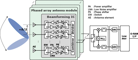
Fig. 1 shows an example of analog type phased-array transceiver. Each antenna element has its own beamforming IC (BFIC) for the control of phase and amplitude. Components like the power amplifier and the low nose amplifier are built into the beamformer. A BFIC for mmW band communication for 5G integrates beamformers for 4 to 32 antenna elements depending on the purpose. While Fig. 1 assumes the use of RF phase shift method, there are reports of choosing LO or IF shift method instead, and the boundary with the modulation-demodulation circuit varies depending on the choice3)4). As to the question of to what extent a phased-array transceiver should include functions of the PHY and MAC layer, the situation varies from case to case among terminal device applications and base station applications, resulting in a wide variety of implementation styles. Each antenna element is connected to a beamformer to enable control of the beam pattern.
3. BFIC and Module Design
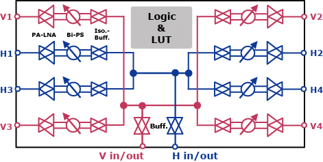
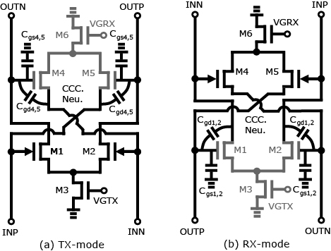
In the developed BFIC, the occupied on-chip area for each beamformer is reduced to half by the bi-directional technique4). Each beamformer in this work consists of a bi-directional gain amplifier, a bi-directional active vector-summing phase shifter, and a power amplifier (PA)–low noise amplifier (LNA) as shown in Fig. 2. A schematic diagram of the bi-directional gain amplifier is shown in Fig. 3. The neutralized bi-directional core contains two differential pairs in the cross-coupling connection. The mode selection of the core is realized by switching the tail transistors M3 and M6. Fig. 3 (a) and (b) further explain the TX- and RX-mode operation of the core. By selecting the same transistor size among M1, M2, M4, and M5, the gate-drain capacitance neutralization could be maintained in both operating modes. Improved amplifier gain and reverse isolation are achieved. In addition, the transmission line (TL)-based passive matching components for the gain amplifier are shared between the TX mode and the RX mode in order to minimize the required chip area. At mmW frequencies, the required matching conditions for the proposed core will not change dramatically during the mode switching. Therefore, same TLs realize low-loss matching in both the TX mode and the RX mode. As a result, a high-performance and area-efficient bidirectional amplifier could be realized.
In an APAA, a number of antenna elements arranged at the pitch of about one-half of the wavelength must be fed signals from a BFIC. Since, in the mmW band, the short wavelength increases losses produced by wiring, BFICs and antenna elements must be placed close to one another as attempts are made to realize a compact, highly integrated module. An APAA module for use at wireless base stations normally has from ten and several to several tens of BFIC to control from 64 to 512 antenna elements. As shown in Fig. 4, the implementation style is largely classified into an antenna on board (AoB) and an antenna in package (AiP).
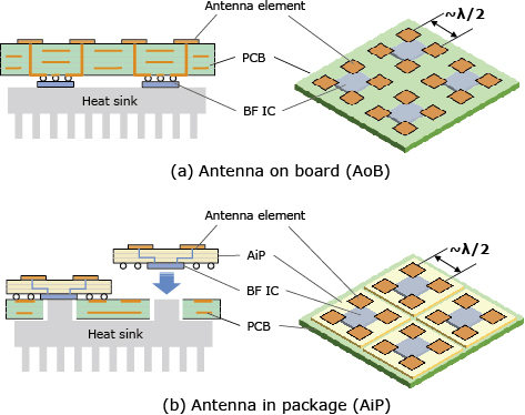
In the case of AoB, antenna elements are mounted on one side of the printed circuit board (PCB) and BFICs on the other side. As the primary advantage, the cost is low because a general-purpose PCB is used. In addition, it is easy to connect a heat sink immediately to the back of the BFIC chips, which are heat generators. This is also a great advantage for wireless base station applications that are prone to the problem of large heat output.
In the case of AiP, antennas are formed within a semiconductor IC package before it is placed on the PCB. AiP has the advantage of fined design rules and high manufacturing accuracy because advanced packaging technology is used. AiP is mostly chosen for the implementation of a relatively small array with 4 to 32 antenna elements. When it is applied to implement a larger array for use at base stations, a tile-like arrangement must be chosen as in the case of the example shown in Fig. 4 (b). High scalability and ease of testing are found to be advantages.
Whether AiP or AoB should be selected depending on the form of phased array equipment in which it is mounted.
4. Implementation and Measurements
A micrograph and a block diagram of the 28-GHz beamformer IC are shown in Fig. 5. Mature 65-nm CMOS technology was utilized, and the chip size was 4 mm × 4 mm. The IC includes 4-channel H-pol. And 4-channel V-pol. transceivers to support dual-polarized MIMO. The element transceiver implements the bi-directional architecture of a frontend amplifier, a variable gain amplifier, and a phase sifter for a compact chip size. The AoB and AiP type phased array antenna modules have been developed using the 28 GHz BFICs as follows.
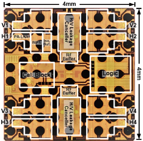
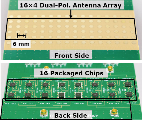
Fig. 6 shows the AoB type phased-array module. Antenna elements form an array at the pitch of 6 mm, which corresponds to 0.56λ, where λ is the free space wavelength for 28 GHz, and the area size of the 16×4 two-dimensional array antenna module is about 3 cm×10 cm. For reducing losses, the wiring between antenna elements and BFICs are designed to be the shortest because a set of four antenna elements is made to connect with one BFIC (as in Fig. 2). The BFICs used for the AoB are fabricated with Fan-in wafer level package (WLP) technology to minimize the implementation size and loss. In over-the-air measurement, a 64-element dual-polarized phased-array module achieves 52.2-dBm saturated effective isotropic radiated power (EIRP). The measured DP-MIMO EVMs are 3.4% with standard-compliant DP-MIMO signals in 256-QAM. The specifics of these BFIC and AoB were reported in Reference 4).
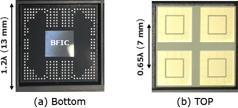
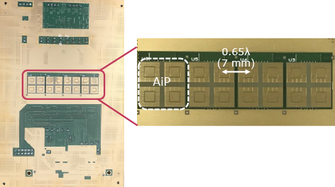
The AiP has 2×2 dual-polarized phased array antennas using chip-last fan-out WLP technology. The size of the AiP is 13 mm × 13 mm × 0.47 mm. 2×2 square patch antennas are formed on the top layer of the RDL. The antenna pitch is 7 mm (0.65λ)(Fig. 7). The four AiPs were mounted on a PCB to form a 8×2 phased array antenna module as shown in Fig. 8. Here, the AiP is designed to be scalable so that the antenna spacing between the adjacent AiPs is kept at 0.65λ.
The OTA measurements were conducted for the fabricated AiP and the phased array module. The AiP was tested in TX mode in a far-field using a vector network analyzer (VNA) and a standard gain horn antenna as a receiver at a distance of 1 m. The beamformer ICs were controlled with FPGA via serial peripheral interface (SPI).
The overall V-pol. EIRP increases along an ideal slope of 6 dB/octave as the number of activated antenna elements increases as shown in Fig. 9, verifying the scalability of the developed AiP. When the 16 antenna elements, i.e., four AiPs, are activated, the peak EIRP reaches 40.5 dBm per polarization.
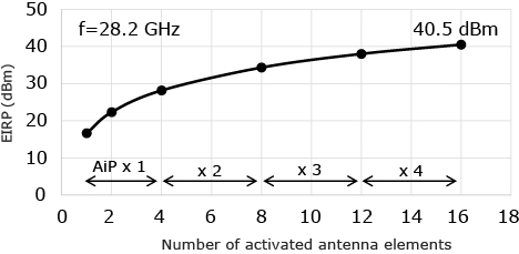
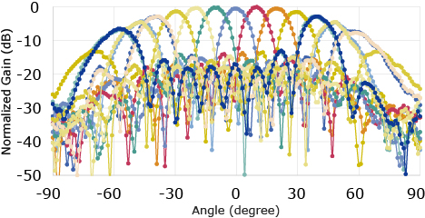
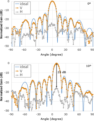
Fig. 10 shows the beam patterns of 8×2 antennas with scan resolution of 1-degree. The 3 dB beamwidth is +/- 40° as well as that of the single antenna. The side lobes are lower than -13 dB. Fig. 11 compares the measured and ideal beam pattern at direction angles of 0° and 10°, respectively. The cross-pol. isolations achieve over 25 dB. It’s due to the antenna configuration and the manufacturing precision of AiPs.
5. Conclusion
This paper described mmW phased-array transceivers used in 5G focusing mainly on IC/module implementation techniques. In the BFIC, area-efficient neutralized bi-directional techniques were used for sharing the circuit chain between TX and RX modes. The two types of antenna modules, AoB and AiP, were developed using the BFICs. We demonstrated a dual-polarized 28-GHz 64-element phased array AoB and a 4-element scalable AiP. These BFIC and phased array module are key technologies for low-cost and compact mmW radio unis in 5G and beyond.
6. Acknowledgement
This work was partially supported by the Ministry of Internal Affairs and Communications in Japan (JPJ000254).
References
- 1)
- 2)KUNIHIEO Kazuaki, OKADA Kenichi: Millimeter-wave CMOS Circuit Technology for 5G, The Journal of The Institute of Electronics, Information and Communication Engineers, Vol.101, No.11, pp.1123-1129, November 2018 (Japanese)
- 3)
- 4)
 J. Pang, et al.: A 28-GHz CMOS Phased-Array Transceiver Based on LO Phase-Shifting Architecture With Gain Invariant Phase Tuning for 5G New Radio, IEEE Journal of Solid-State Circuits, Vol.54, No.5, pp.1228-1242, May 2019
Copyright(C)2022 IEICE
K. Okada, J. Pang, A. Shirane, N. Oshima, K. Kunihiro: Millimeter-wave Phased-array Transceiver for 5G and Beyond, Journal of IEICE, Vol. 105, No.8, pp.706-712, August 2022
Copyright(C)2022 APMCy
N. Oshima, S. Hori, J. Pang, A. Shirane, K. Okada, K. Kunihiro: A Low-Profile, Scalable 28-GHz Phased Array Antenna in Fan-Out Wafer-Level Package for 5G Communication, 2022 Asia-Pacific Microwave Conference (APMC), pp.359-361, December 2022
Authors’ Profiles
OSHIMA Naoki
Professional
Global Mobile Solution Department
Professional
Global Mobile Solution Department
HORI Shinichi
Professional
Wireless Access Development Department
Professional
Wireless Access Development Department
PANG Jian
Specially Appointed Associate Professor
Tokyo Institute of Technology
Specially Appointed Associate Professor
Tokyo Institute of Technology
SHIRANE Atsushi
Associate Professor
Tokyo Institute of Technology
Associate Professor
Tokyo Institute of Technology
OKADA Kenichi
Professor
Tokyo Institute of Technology
Professor
Tokyo Institute of Technology
KUNIHIEO Kazuaki
Senior Professional
Wireless Access Development Department
Senior Professional
Wireless Access Development Department