
Global Site
Breadcrumb navigation
Carbon Nanotube
Featured TechnologiesSeptember 1, 2017(Rev. September 24, 2024)
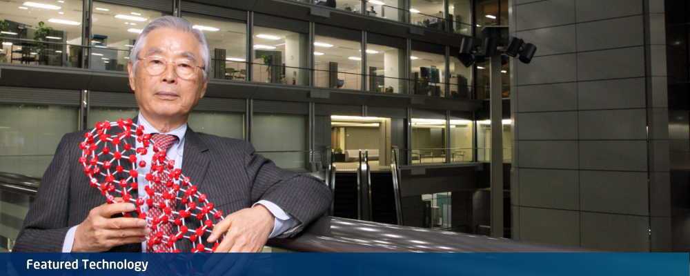
"Carbon nanotube" was discovered in 1991 by Sumio Iijima, a senior research fellow at NEC (then Chief Researcher at NEC's Fundamental Research Laboratories). NEC is conducting research and development targeting next-generation transistors using carbon nanotubes.
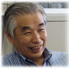
Here, Dr. Iijima looks back on his history as a researcher, and talks about the future of carbon nanotubes.
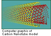
Computer Graphic of Carbon Nanotubes
Please view this page in a broadband environment.
In some cases this page may be difficult to view in a narrowband environment.

1. What are carbon nanotubes?
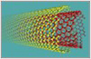
A "Carbon Nanotube" is a tube-shaped material, made of carbon, that has a diameter measuring on the nanometer scale. A nanometer is one one-billionth of a meter, or about one ten-thousandth of the thickness of a human hair. The graphite layer appears somewhat like a rolled-up chicken wire with a continuous unbroken hexagonal mesh and carbon molecules at the apexes of the hexagons. In some cases, the hexagons are arranged in a spiral form. The pattern is reminiscent of the Japanese art of bamboo basket weaving ("Takekago").
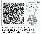
Solid state carbon has been known to appear in four basic forms: "diamond structures,""graphite structures,""non-crystalline structures" (such as charcoal), and "fullerene molecules" such as C60, which is comprised of 60 carbon molecules clustered in a soccer ball shape. Fullerene molecules were discovered in 1985. The carbon nanotubes that I discovered thus became the fifth type of solid state carbon.
The carbon nanotubes that I found in 1991 had multiple walls, but in 1993 I discovered single-wall carbon nanotubes that were one nanometer thick and several tens of nanometers long. (These were discovered separately at IBM around the same time.) Later, our group promoted research into material characterization and computational physics, and this became the forerunner of carbon nanotube research. In 1996, Thomas Ebbesen's group at the Princeton NEC Research Institute succeeded in measuring the electrical characteristics of carbon nanotubes.
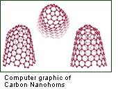
Then, in 1998, during the Japan Science and Technology Corporation (JST) International Cooperative Research Project "Nanotubulites," I discovered single-layer graphite shaped like a tube with a closed end, which was later to be given the name "Carbon Nanohorn." These carbon nanohorns were comprised of carbon collected in the shape of an bull's horn covered over with a hood.
Carbon nanotubes have many structures, differing in length, thickness, type of spiral, and number of layers. Although they are formed from essentially the same graphite sheet, their electrical characteristics differ depending on these variations, acting either as metals or semiconductors.
2. The discovery of carbon nanotubes - Guided by serendipity
It all started in 1971, when I developed the world's first high-resolution electron microscope at Arizona State University. In the 1970s, I had the opportunity to study many different types of carbon materials. In 1980, I announced that I had seen "spherical graphite*," in a research paper I wrote related to carbon. I noticed that among the various forms of graphite, there were "onion-shaped" particles about 0.8 - 1 nanometer in diameter, and commented in my paper that "In order to explain the onion-like formation of this spherical graphite, in addition to hexagonal carbon graphenes**, 12 pentagonal graphenes were also required." This onion-like structure is in fact the fullerene (carbon-60 or C60) discovered in 1985 by Harold W. Kroto, Richard E. Smalley, and Robert F. Curl. At the time of that discovery, this fact was overlooked.
- *Graphite is a flat crystal layer in which carbon molecules are arranged in a hexagonal shape. It is used in pencil lead and as a fiber in golf clubs and tennis racquets.
- **"Hexagonal Graphene" refers to the state in which the molecules are arranged at the six apexes of a hexagon.
Based in part on this experience, when I heard about the discovery of C60 in 1985, I thought to myself, "So THAT was the onion-like structure that I saw." At the same time, I gained a new interest in the ways in which molecular structures with a perfect symmetrical shape like C60 are created.
From 1987, when I began working at NEC's Fundamental Research Laboratories, I decided to once again study these "onions" to reconfirm the research that I had conducted five years before.
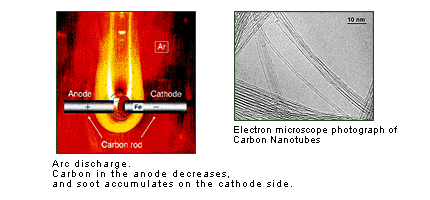
Shortly after I began studying these onion structures, however, my attention was drawn not to C60, which demonstrated this onion structure, but rather to a needle-shaped material that appeared nearby. In the large-scale synthesis, using a method announced in 1990, C60 is generated using discharge from two carbon electrode rods (the arc discharge method). Within the soot that built up above the negative carbon pole, however, I found a needle-shaped material that had never been seen before. This needle-shaped material is the material to which I later gave the name "carbon nanotube."
→ See the Story Behind the Name
At the time, this discovery was seen as something of a "product of coincidence", but I prefers to think of this as necessity rather than coincidence. The thing that became clear to me when I saw this needle-shaped material was the connection between two factors: that one part of the theme of my doctoral thesis was the "needle crystals of silver," and that the asbestos which an assistant professor in the same laboratory at that time had been studying using an electron microscope had a tube-like crystal structure. In other words, that discovery was not simply "coincidence" - it was the power of "serendipity."
"Serendipity" is defined as "the ability to find valuable things," or "the faculty of discovery." I believe that I naturally came to have this ability through skills in using electron microscopes, which I had cultivated over many years, through my continued experience in working with carbon and my involvement with mineralogy in the United States, and, more than anything else, my strong determination to pursue research in unknown materials, for which the structures had not yet been clarified. Carbon nanotubes are nothing more than one of the things that I discovered through this continued process of searching for the truth.
→ See origin of the term "serendipity"
The Story Behind the Name
For some time after the discovery, I had used the term "micro-tubule," referring to microscopic tubes found in living organisms, and it was featured in the journal "Nature" on two occasions using this term. The Director of the Fundamental Research Laboratories at the time, Dr. Hiroyoshi Rangu (currently a Professor at the Tokyo University of Agriculture and Technology) said, "Don't you think you should pick a name that will be recognized worldwide? The name is very important, you know." I was in full agreement with Dr. Rangu, and decided upon the name "carbon nanotubes."
"Fullerenes" were named after the American architect Richard Buckminster Fuller, but the name "carbon nanotube" was selected from among several candidates, including "microtubules," which I used in my first paper, and "tubulin," originally the name of a protein, as well as "NEC tubes" and "Iijima tubes." Some people expressed the opinion that although the tubes were nano-sized, using "micro" was inappropriate, so I gave up on "microtubules," and I also decided against "Iijima tubes" because I felt embarrassed about using my own name. This is a type of "carbon," with a size on the "nano" scale, and shaped like a "tube" - so I settled on "carbon nanotubes."

Origin of the term "serendipity"
It is said that the English author Horace Walpole (1717-1797) coined the term "serendipity" in a letter to a friend written in 1754. He based the term on the title of a Sri Lankan fairy tale he had read, called "Three Princes of Serendip," Serendip being the former name of Sri Lanka. It was a story of three princes who "were always making discoveries, by accidents and sagacity, of things which they were not in quest of." He thus used the term to describe unexpected but valuable discoveries.
3. Applications of carbon nanotubes
Carbon nanotubes are expected to become a key material in ultrafine devices of the future, because of their unique electrical characteristics, and their extraordinarily fine structure on a nanometer scale. Other merits offered by carbon nanotubes are light weight, extremely high mechanical strength (they have larger tensile strength than steel), their ability to withstand extreme heat of 2000°C in the absence of oxygen, and the fact that they emit electrons efficiently when subjected to electrical field. Currently, research is being conducted throughout the world targeting the application of carbon nanotubes as materials for use in transistors and fuel cells, which we are currently working on, as well as big TV screens, ultra-sensitive sensors, high-resolution AFM probes, supercapacitor, transparent conducting film, drug carrier, catalysts, and composite material.
In 1999, in collaboration with JST, we developed a nanostructure fabrication technology that uses carbon nanotubes as key material for electronic devices on the nanometer level, and succeeded in connecting carbon nanotubes with other materials using a process of "solid-chemical reaction". In 2001, NEC and the Japan Science and Technology Corporation and the Institute of Research and Innovation succeeded in developing the world's first compact fuel cell for mobile devices, which used carbon nanotubes for the electrodes. In September 2003, we developed a prototype of a carbon nanotube transistor that is more than ten times faster (based on mutual conductance) than silicon MOS transistors (announced at the 2003 International Conference on Solid State Devices and Materials (SSDM) as part of a project by the New Energy and Industrial Technology Development Organization (NEDO)).
In Sept. 2004, NEC Corporation announced the development of a diameter/position-controlled carbon nanotube ("CNT") growth technique. This technique will provide a practical method for controlling the position and diameter of CNT. NEC expects this result will promote the research and development of high-performance CNT electronic devices. In addition, NEC announced the successful development of a carbon nanotube (CNT) transistor using a coating process in 2008. In 2009, NEC announced the successful demonstration of the fully printed CNT transistor, and announced the world's fastest operation speed demonstrated using printed CNT transistor in 2013. NEC will continue to work on advancements in CNT control technology, electric characteristic control, device structure design, and fabrication process development with the aim of realizing a CNT transistor by 2015.
In 2005, NEC demonstrated the possibility of applying carbon nanohorns to the drug delivery systems, in cooperation with JST and Cancer Institute. At present, this activity was transferred to AIST, and further R&D towards practical use is continued.
-
- 25 Jun. 1991
-
NEC Discovers Helical Structure “Carbon Nanotube”
- Nov. 1991
-
Nature, Vol.354 No.6348 p.56
“Helical microtubules of graphitic carbon” - Jan. 1993
-
NEC Succeeds in Developing Carbon Nanotubes Filled With Different Materials
Nature, Vol.361 No.6410 p.28
"Capillarity-induced filling of carbon nanotubes" - Jun. 1993
-
The Discovery of Single-shell Carbon Nanotubes
Nature, Vol.363 No.6430 p.17
"Single-shell carbon nanotubes of 1-nm diameter" - Jul. 1996
-
NEC Succeeds in Measuring Electrical Properties of Individual Carbon Nanotubes (NEC Corporation & NEC Research Institution Inc.)
Nature, Vol.382 No.6586 p.54
“Electrical conductivity of individual carbon nanotubes”
- Mar. 1998
-
The Discovery of Carbon Nano-horns
(JST*・International cooperative research project, “Nanotubulites Project”)
JST:Japan Science and Technology Corporation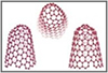
- Aug. 1999
-
Chem. Phys. Lett., 309, p.165
"Nano-aggregates of single-walled graphitic carbon nano-horns" - Sept. 1999
-
NEC Develops Nano-Fabrication Technique for Carbon Nanotubes
(NEC & Japan Science and Technology Corporation-International Cooperative Research Project “JST-ICORP”) - Aug. 2001
-
NEC uses Carbon Nanotubes to Develop a Tiny Fuel Cell
for Mobile Applications (NEC, JST, Institute of Research and Innovation ) - Sept. 2001
-
Tsukuba Symposium on Carbon Nanotubes
- Nov. 2002
-
NEC Succeeds in Operating Top-Gate Carbon Nanotube Transistors for LSI
- Feb. 2003
-
Fuel Cell Powered Notebook PC (Exhibited at “Nano Tech 2003”)
- Jun. 2003
-
Unveiling of Notebook PC with Built-in Fuel Cell
- Sept. 2003
-
Smaller Fuel Cell for Notebook PCs
(Exhibited at “WPC EXPO 2003”)
Tests Verify Carbon Nanotube Enable Ultra High Performance Transistor - Sept. 2004
-
Realizes Control of Position & Diameter of Carbon Nanotube 発
- Oct. 2004
-
Fuel Cell Powered Notebook PC (Exhibited at “WPC EXPO 2004”)

- Nov. 2005
-
Carbon Nano-horn Drug Delivery System
- Feb. 2008
-
NEC Succeeds in Fabrication of CNT Transistor Using Coating Process
- Feb. 2009
-
NEC Successfully Produces CNT Transistors through Specialized Printing Processes
- Apr. 2012
-
Development of uniform carbon nanotube thin-film transistors printed on flexible plastic films
- Sept. 2013
-
World’s fastest operation speed demonstrated using printed CNT transistor
- Jun. 2016
-
NEC discovers "carbon nanobrush," the world's first fibrous aggregate of carbon nanohorns
Advanced materials 33/2016
“Preparation and Characterization of Newly Discovered Fibrous Aggregates of Single-Walled Carbon Nanohorns“ - Feb. 2018
-
NEC, AIST and Meijo Nano Carbon Develop a Technology for Manufacturing High Purity Semiconducting CNT Ideal for Printed Electronics
- Apr. 2023
-
NEC develops the world's first highly sensitive uncooled infrared image sensor utilizing carbon nanotubes
4. The future of carbon nanotubes
Currently, we are gaining a greater understanding of the electrical characteristics of carbon nanotubes through both theoretical and experimental means.
Research is moving forward in the field of fabrication methods, but many have said that it is difficult to produce long carbon nanotubes formed basically from hexagonal graphenes, because in the process of generating these nanotubes, pentagonal and heptagonal graphenes are also created, resulting in tubes with closed ends or with ends that spread out. Progress has been made in technologies for creating long tubes, however; for example, in April 2003, American researchers announced that they had created a carbon nanotube with a length of six millimeters. Our group has set a target for the large-scale production of carbon nanohorns, and has already entered the implementation phase.
However, there are still several remaining issues as regards CNT synthesis. For example, we still cannot control the chirality of the tube, which determines the electrical property of CNT. Also, some have asked whether it will be possible to use carbon nanotubes in hydrogen storage materials; although methane is absorbed effectively, we have recently found that hydrogen storage is problematic.
NEC has succeeded in developing the world's first high-sensitivity uncooled infrared image sensor that uses high-purity semiconducting carbon nanotubes (CNTs) in the infrared detection area. This was accomplished using NEC’s proprietary extraction technology. NEC will work toward the practical application of this image sensor in 2026.
Globally, alongside the establishment of mass production methods for carbon nanotubes, the development of technologies necessary for industrial expansion continues to accelerate. These include techniques for high-precision separation of semiconducting and metallic types of CNTs, as well as technologies to control their dispersion and alignment. In addition to electronic components, electronic devices, battery materials, and functional composite materials, further expansion of applications is anticipated.
5. About Myself
In "About Myself," we introduce the origins of NEC's top researchers, and look at some of the many transformations that their research activities undergo. For some time now, we have heard warnings that more young Japanese are moving away from the sciences, or that it is experiencing a "hollowing out of the production industry." Through these researchers' messages, we hope that readers will feel a greater familiarity with science and technology, as well as a deeper interest in these fields. In this edition, we have a message from Dr. Sumio Iijima.
- In my youth
- First meeting with the electron microscope, and acquisition of a specialty
- In the United States
- Why I joined NEC after returning to Japan
- The "Friday Evening Discourse"
- The "Friday Evening Discourse"
- To the younger generation
- To people wishing to become involved in the sciences
- References
In my youth
I am often asked what I was like when I was a child. Stated very simply, I loved nature. When I was little, I took advantage of every opportunity to come in contact with nature - I collected plants and insects, I fished, and I kept a menagerie of small animals, including pigeons, rabbits, snakes, frogs, and crabs. I learned many things from my experiences with nature, and I believe that this helped me to develop both sensitivity and insight. In high school and university, I was in the mountaineering club and the music club, and spent my youth exploring nature and challenging the limits of my creativity.
First meeting with the electron microscope, and acquisition of a specialty
Upon my graduation from the University of Electro-Communications, Faculty of Communications, instead of going into engineering, I changed directions into the field of science. Although I managed to get into the Graduate School of Physics at Tohoku University, I had come from a different field at a different university and so my laboratory placement was decided immediately after my interview. It just so happened that I was assigned to the laboratory of Professor Tadatoshi Hibi, who was a pioneer in electron microscope research.
It wasn't that I had a particularly strong desire to do research with electron microscopes at the time, but I found that I was perfectly suited to research in this field. After I finished my Ph.D., I spent two years as a Research Associate in the Research Institute for Scientific Measurements at Tohoku University and 12 years as a Research Associate at Arizona State University in the United States. During that time, I developed a new electron microscope that was the first in the world to show the structure of materials at the atomic level. This field that I had dived into head first - the use of electron microscopes to explore physical phenomena and structures of materials at the nanometer level - came to be my specialty.
So it was that my meeting with the electron microscope determined my path in research, but perhaps this meeting was in fact more coincidence than "serendipity." Nevertheless, it is true that the changes in that path, and the fact that I dove into new fields, was a result of my determination to find something, and I believe that there was something working here other than mere coincidence.
In the United States
I spent the years from 1970 to 1982 at Arizona State University in the United States. (In 1979, I stayed in England as a visiting senior scientist at the University of Cambridge.) In a word, one could say that these years represented my "apprenticeship." The most important thing that I learned while in the U.S. was "Don't do what others have done."
As a result of this approach, in 1971, I developed a high-resolution electron microscope and became the first in the world to directly observe metal atoms in the crystal lattice of titanium-niobium oxide. In 1973, I used the same high-resolution electron microscopy to record images of point defects in crystals through resolution at the atomic level. In 1977, I succeeded in the imaging of individual tungsten atoms, and was told that I had achieved the dream held by researchers since the invention of the electron microscope in 1932 - that of actually seeing a single atom.
Why I joined NEC after returning to Japan
I returned to Japan in 1982, and participated in the first research project of the Research Development Corporation of Japan (now JST), developing a new high-resolution electron microscope. Then, in 1984, I discovered the phenomenon of "Structural instability of ultrafine particles of metals," in which the atoms of metals move about like amoeba. For the five years after my return to Japan, from 1982 to 1987, I devoted my efforts mainly to research in ultrafine particles.
I entered NEC after this period, in 1987. About the time when I was thinking that I wanted to develop a new high-resolution electron microscope that could operate in an extremely high vacuum, NEC expressed a similar interest in the development of such an electron microscope. I thus began my first experience as a company employee at the age of 48. Another reason that I dove into fundamental research in a company was that electronics laboratories have unique materials produced using expensive equipment that cannot be made in universities, and I was sure that these materials would become the basis for exceptional research results using electron microscopes. The third reason was that I wanted to test my own abilities - I thought to myself, there is no reason why I can't conduct fundamental research even in a company laboratory. This was because I believe that when laboratories at universities and companies compete in basic research and grow stronger through this friendly rivalry, the result will be that fundamental research will provide support for a wide range of researchers - the healthiest pattern for the research field. Of course, all this has to take place within the scope that the economic environment will allow. I liked NEC's management policy, which was based on the approach of "broad proliferation of science and technologies, and the creation of new value," and of "giving back to society."
It took about two years after I entered NEC, but I was finally able to achieve my goal of undertaking world-leading development of microscopes. Looking back on it now, the first paper I wrote after joining NEC was about C60. I really feel that there was a connection there.
The "Friday Evening Discourse"
Even after discovering carbon nanotubes, my own lifestyle and style of research didn't change in any particular way. If I had to say something, I'd say it was that I became so busy that I had very little time for myself. I really believe (at least I'd like to believe) that my directions in research and my curiosity about things in general, are the same now as they ever were.
One exception, perhaps, is the presentation that I made in May 1997 at the Friday Evening Discourse, which is held by the Royal Institution in England. I have given many presentations in the past, but this one in particular remains with me as a very valuable experience that impressed upon me the tradition of sciences in England.
The discourse has no prologue or introductions; it begins promptly at 8:00 p.m. with the sound of a bell. The bell rings once more an hour later, and the discourse must then be ended just as promptly, even if the speaker has not yet completed the presentation. This is the traditional style of the Friday Evening Discourse. In my case, I completed my presentation three seconds ahead of time, and the bell rang just as I was taking a breath after finishing. The timing was worthy of being written up in the Guinness Book, and everyone in attendance responded enthusiastically.
During my discourse, I made the following comment: "When I am asked about the practical value of carbon nanotubes, I respond with the same reply that the great English scientist Michael Faraday gave to the Chancellor of the Exchequer (the Minister of Finance at the time): 'One day, Sir, you may tax it.'" This comment also won a rousing response. I used this metaphor to make the point that carbon nanotubes offer so many merits that one day there may be a tax levied on their use, but I think perhaps the idea is even more appropriate now than it ever was.
The "Friday Evening Discourse"
The Friday Evening Discourse was founded in 1825 by Michael Faraday, the father of electromagnetics, with the goal of introducing advanced sciences to the general public in an easy-to-understand format. Since that time, authoritative discourses have been held in the very same location, at the Royal Institution in London.
Twenty times each year, on Friday evening, the world's top researchers give easy-to-understand presentations of their recent results, focusing mainly on experiments, not only to specialists but to a wide range of non-specialist intellectuals including doctors, lawyers, and representatives of the Royal Family. It is a very prestigious affair, in which speakers and listeners alike are required to wear black ties; a scene from the Discourses even appears in the design on one of the notes currently used in British currency.
A long list of Nobel-class scientists have given presentations at the Friday Evening Discourse, including James Clerk Maxwell, Lord Rayleigh, Sir James Dewar, Alexander Fleming, J.J. Thomson, Pierre Curie, Irving Langmuir, and Sir Harold Kroto. Dr. Iijima became the fifth Japanese person to give a presentation at the Friday Evening Discourse, following Makoto Kikuchi (Sony; 1984), Iwao Fujimasa (Tokyo University; 1994), Akira Tonomura (Hitachi; 1994), and Kuniaki Nagayama (Tokyo University; 1997).
To the younger generation
I often use the word "Serendipity," because I believe that in order for coincidences to happen, the process leading up to it is very important. The ability to see things correctly is nurtured through day-to-day observation. When I see so many stories in the news recently about violent crimes, I can't help but think that as children, these people were never trained to think for themselves and to act correctly. "Excessive service" is rampant in Japan today. For example, consider the announcements you hear on the train platforms. This is a very helpful announcement, which tells us, "For your safety, please wait behind the white line." But really, the passengers should be able to make this judgment for themselves. If we are raised in a world where someone will always give us the answer even if we don't think for ourselves, then we will never learn the skills required to live independently. If children in modern Japan were made to participate in a "survival game," I doubt very much that even one would remain standing at the end. This is the responsibility of the adults in our society. I would like to see more people coming in contact with nature, and living their lives thinking for themselves, and acting accordingly.
I think that one of the reasons for the warnings we have heard in past years that Japan is "losing its connections with science" is a lack of sensitivity and observation skills, which are learned through contact with nature. Research can be undertaken in any kind of environment, as long as you have the interest. I believe that true education means fostering the ability to be interested in something.
To people wishing to become involved in the sciences
I mentioned earlier that the key lies in "not doing what others have done," but "doing what others have not done" demands a great deal of motivation. Where does this motivation originate? This is a difficult question. Perhaps it is the training to see things with a broad perspective, and see through to the truth. We have a limited time to work with, so we want to find a research theme that will have impact. You may think it is difficult to continue fundamental research in a company, which must emphasize profits. In practical terms, the key lies in whether the researcher has the ability to see what lies ahead, and whether that researcher's manager is able to see the value in that future. Of course, if that seed stays a seed, never bearing fruit, then one must have the courage to quit as well. This can be extremely difficult, however, if a large amount of money has already been invested in that research.
I would like to ask the young people in Japan to strive for research results that Japan can be proud of, regardless of whether you are doing research in a company, a university, or some other research environment. Without this pride, when we take our place on the global stage, we cannot ever feel totally relaxed. You must have the confidence to be able to say, "I am creating Japanese culture." For example, I believe that research and fabrication technologies using electron microscopes - my own specialty - are something we can be proud to offer to the world. I urge you to go out and create sciences and technologies that you can be proud of presenting on a global stage.
References
-
"The Challenge of Carbon Nanotubes"; Iijima, S., Iwanami Shoten, Published Jan. 1999 (in Japanese)
 National Institute of Advanced Industrial Science and Technology (AIST) Homepage
Related Link
- February 8, 2018 Press Releases
NEC, AIST and Meijo Nano Carbon Develop a Technology for Manufacturing High Purity Semiconducting CNT Ideal for Printed Electronics
- Meijo Nano Carbon to begin marketing semiconducting CNT from FY2018 - - February 8, 2018
Development and practical application of separation technique for metal and semiconductor carbon nanotubes - NEC begins marketing "Carbon Nanohorn"
- Wide ranging uses include medical innovations and capacitor enhancement -