
Global Site
Breadcrumb navigation
Development and practical application of separation technique for metal and semiconductor carbon nanotubes
Featured TechnologiesFebruary 8, 2018

What are carbon nanotubes?
Carbon nanotubes (CNTs) are nanocarbon material discovered in 1991 by Sumio Iijima of NEC.[1] A CNT is a tube-shaped structure made of cylindrically-arranged graphene sheets. CNTs can be categorized into single-walled carbon nanotubes (single-walled CNT)[2], which have one graphene sheet layer, double-walled CNTs, and multi-walled CNTs. Single-walled CNTs have different electrical properties based on the chirality of the cylindrical rolling. As one-third of the structure has metallic properties while two-thirds have semiconducting properties[3], any application as channel materials for field-effect transistors requires the development of a separation technique.
Ever since the technique to monodisperse individual single-walled CNTs into a solution[4] was established, many researchers have proposed separation approaches for single-walled CNTs. As examples of techniques to separate metal and semiconductor sheets, there are the density-gradient centrifugation[5] and gel electrophoresis[6].
The current method used for the separation of single-walled CNTs adopts surfactants containing sodium or other metal ions as dispersant when dispersing the CNT into the solvent. However, this dispersant can cause instability in device operations or degradation in performance when semiconducting CNTs are used as a material for electronic devices, such as when it is used as a channel in a field-effect transistor (FET) (area where the current passes between the transistor's drain and source electrodes). This means that if higher-purity semiconducting CNTs can be acquired without using an ionic surfactant, FET devices with superior stability can be produced.
Electric-field-induced layer formation (ELF) method
The ELF is a method developed by Kazuki Ihara and others at NEC. With this method, single-walled CNTs can be monodispersed by a non-ionic surfactant (Fig.1), and the dispersions are loaded in a separator where voltage is applied to its top and bottom electrodes, separating metallic and semiconducting CNTs by means of carrier-free electrophoresis (Fig.2(a))[7-8]. When single-walled CNTs are dispersed using a non-ionic surfactant, the semiconducting CNT micelles have a negative zeta potential while the metallic CNT micelles have a positive (reversed-sign) zeta potential. Therefore, applying an electric field to the single-walled CNT dispersions electrophoreses semiconducting CNT micelles to the anode and metallic CNT micelles to the cathode. Finally, a concentration of semiconducting CNT forms around the anode and a concentration of metallic CNT forms around the cathode in the separation chamber (Fig.2(a)). Fig.2(b) shows the collected metallic and semiconducting CNT dispersions. The ELF method can also be used to separate various commercially-available single-walled CNTs by controlling the zeta potential of the single-walled CNTs.
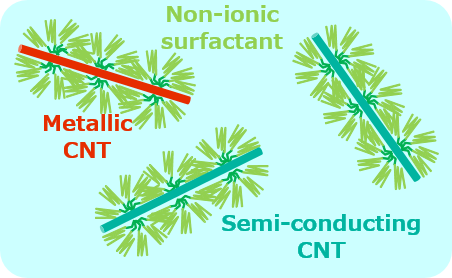
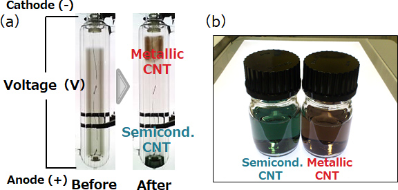
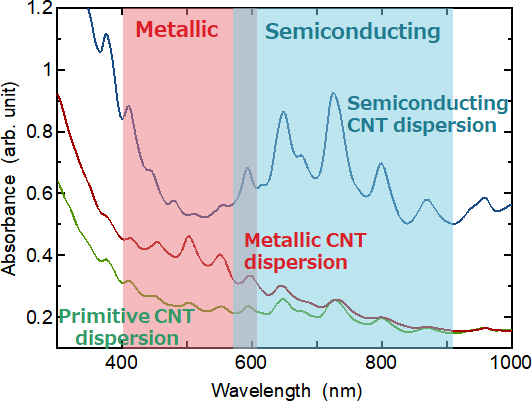
Fig.3 shows the optical absorption spectra of CNT dispersions before (dispersed by non-ionic surfactant) and after separation by the ELF method. Red and blue parts respectively indicate the absorptions deriving from metallic and semiconducting CNTs. After separation, the semiconducting CNT dispersion shows almost no metallic CNT-based absorption, but rather a noticeably strong semiconducting CNT-based absorption. The area ratio of resonance Raman spectra for these dispersions turned out a 99% semiconducting CNT for the separated dispersion.
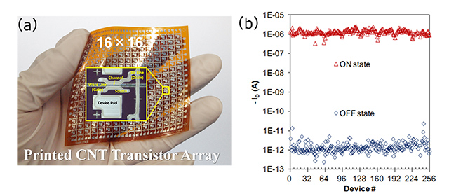
We created a thin-film transistor using a semiconducting CNT dispersion produced using this technique and evaluated its device properties. Fig.4(a) shows a flexible thin-film transistor (16 x 16) with CNT ink applied to each channel. Fig.4(b) shows the plotting of ON/OFF status of each TFT device (ON: carrying current, OFF: no current). This plot shows a successful acquisition of excellent FET characteristics of 106 ON to OFF ratio. The travel rate was 4.1 cm²/Vs, which is more than 10 times that attainable by amorphous silicon. The above demonstrated the feasibility of the production of high-performance devices with reliable performance, having good uniformity with complete ON/OFF separation. We also obtained good results in the operation test of pressure sensor sheets of this size[9].
References
-
Iijima, S., Helical Microtubulets of Graphite Carbon. Nature 354, 56-58 (1991).
-
Iijima, S. and Ichihashi, T. Single-Shell Carbon Nanotubes of 1-nm Diameter. Nature 363, 603-605 (1993).
-
Saito, R., Fujita, M., Dresselhaus, G. and Dresselhaus, M. S., Electronic structure of chiral graphene tubules. Appl. Phys. Lett. 60, 2204-2206 (1992).
-
O'Connell, M. J., Boul, P., Ericson, L. M., Huffman, H., Wang, Y., Haroz, E., Kuper, C., Tour, J., Ausman, K. D. and Smalley, R. E., Reversible water-solubilization of single-walled carbon nanotubes by polymer wrapping. Chem. Phys. Lett., 342, 265-271 (2001).
-
Chattopadhyay, D., Galeska, I. and Papadimitrakopoulous, F., A Route for Bulk Separation of Semiconducting from Metallic Single-Wall Carbon Nanotubes. J. Am. Chem. Soc. 125, 3370-3375 (2003).
-
Tanaka, T., Jin, H., Miyata, Y., Fujii, S., Suga, H., Naitoh, Y., Minari, T., Miyadera, T., Tsukagoshi, K. and Kataura, H., Simple and Scalable Gel-Based Separation of Metallic and Semiconducting Carbon Nanotubes. Nano. Lett. 9, 1497-1500 (2009).
-
K. Ihara and F.Nihey, Separation Method and System for Nanocarbon Materials. Patent No.5541283.
-
K. Ihara, H. Endoh, T. Saito and F. Nihey, Separation of Metallic and Semiconducting Single Wall Carbon Nanotube Solution by Vertical Electric Field, J. Phys. Chem. C, 115, 228827 (2011).
-
H. Numata, S. Asano, F. Sasaki, T. Saito, F. Nihey, H. Kataura, Adhesion property of carbon nanotube micelles for high-quality printed transistor, Proc. Int. Conf. IEEE-NANO 2016, 849.
- ※The information posted on this page is the information at the time of publication.