
Global Site
Breadcrumb navigation
Key Functions
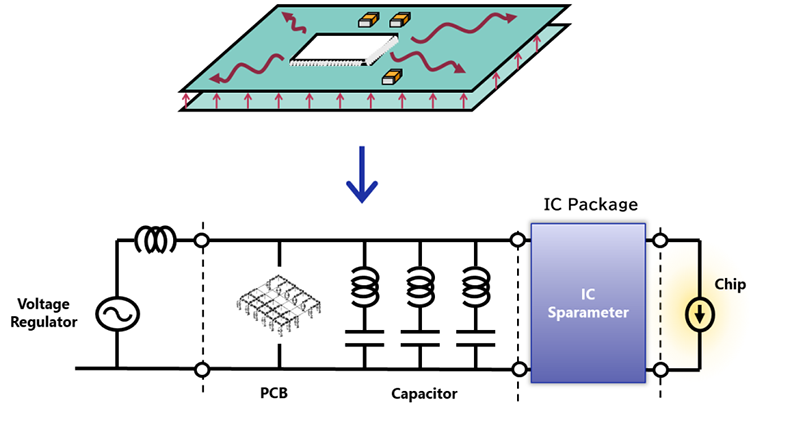
PIStream can support PCB design controlling power integrity (PI) by reducing input impedance and transfer impedance. PI problems occur when IR drop (voltage drop) relevant to IC power consumption in the Power Distribution Network (PDN) occur. The following three key features support your PI design.
1. Input Impedance Analysis
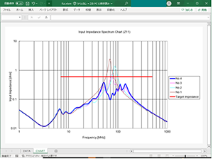
PIStream calculates input impedance and helps you meet your target impedance by adding de-caps, changing the capacitor location, and changing the power plane thickness and shape.
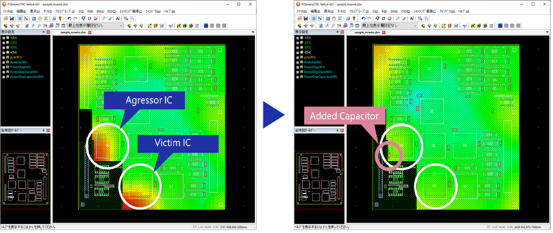
This analysis shows the Z11 effect from an aggressor IC and allows you to consider optimal capacitor position by trial-and-error to keep input impedance below the target impedance.
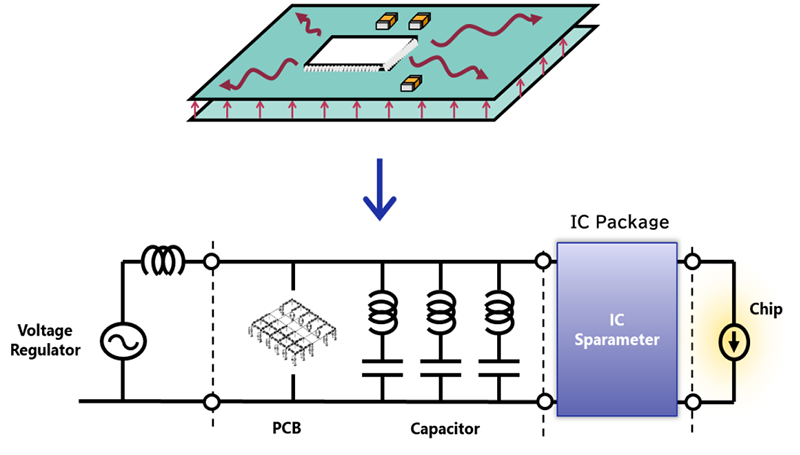
The following figure shows the input impedance (Z11) structure.
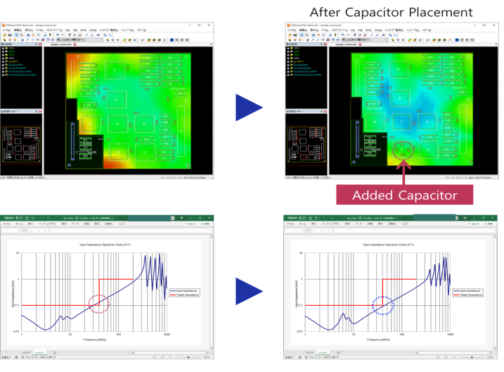
(1) Countermeasure by Input Impedance Analysis
Case 1: Target impedance achieved by adding capacitors around target IC.
Adding capacitors around the red area near the target IC keeps the input impedance below the target impedance. You will be able to optimize capacitor location from this analysis.
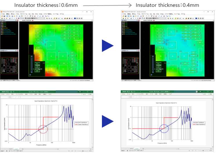
Case 2: Target impedance achieved by changing thickness between power and GND plane.
This example shows that a thinner insulator thickness helps keep the input impedance below the target impedance.
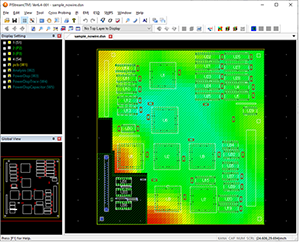
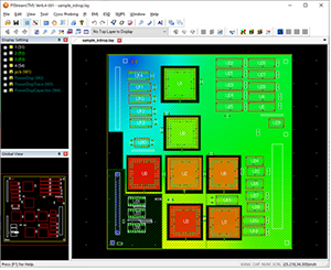
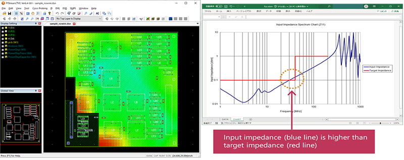
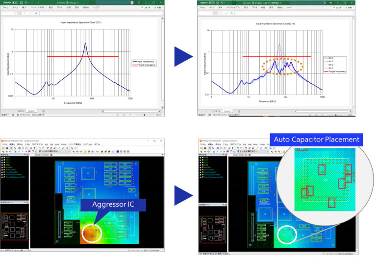
(2) Auto Capacitor Placement
This function selects optimum capacitors for resonance frequency and automatically places them near IC power pins. The following figure shows the effect before and after running the auto capacitor placement function.
As shown, the input impedance is above the target impedance before running this function. After it is run, eight capacitors are added around the IC power pins and color gradation turns to blue.
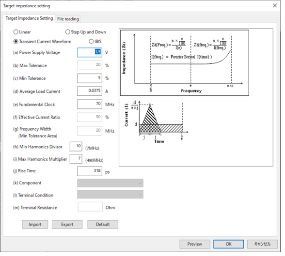
(3) Target Impedance Setting for Input Impedance Analysis
This GUI lets you to enter the allowable maximum impedance value supplied by IC venders. You can also import a CSV file into this GUI.
This setting will appear as a red line as a reference impedance value in the input impedance analysis result.
2. Transfer Impedance Analysis
PIStream calculates transfer impedance to avoid noise transition to other ICs and internal RF interference.
The following figures show the results of transfer impedance analysis.
This function allows you to consider noise distribution caused by the power source (aggressor) IC. A hot area means a high transfer impedance area, and when the aggressor IC consumes a current, it indicates a huge voltage drop (IR drop) has occurred. To avoid such voltage drop, you can put a capacitor on the red area. By doing this, the red area turns to blue and you will be able to confirm if the transfer impedance has been reduced and the noise distribution suppressed.
This analysis shows the Z21 (Transfer Impedance) effect using a color gradation map.
Transfer impedance is calculated by power noise emission from the power source IC.
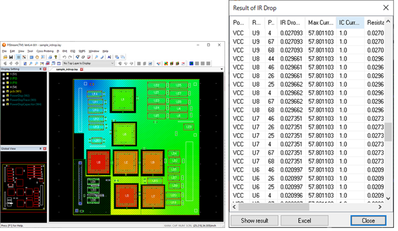
3. DC Analysis (IR Drop)
PIStream also calculates IR Drop and displays color gradation as well as the IR Drop value for each IC.
Contact