
Global Site
Displaying present location in the site.
Reducing the Power Consumption and Increasing the Performance of IoT Devices by Using NanoBridge-FPGA
The NanoBridge-FPGA, a field programmable gateway array incorporating NEC's original NanoBridge metal atom migration-type switch, offers higher power efficiency and faster processing speed while achieving excellent durability against radiation and high temperature. That combination of reduced power consumption and increased performance makes the NanoBridge-FPGA suitable for application in a wide spectrum of fields. Featuring higher power efficiency than a CPU, an FPGA is a group of integrated circuits that facilitate hardware (circuit configuration) switching using semiconductor switches and memory modules. The new NanoBridge FPGA ramps up that power efficiency of the FPGA by replacing these semiconductor switches and memory modules with the space-saving NanoBridge. This paper discusses the operating principle of the NanoBridge, the internal construction of the NanoBridge-FPGA, and compares its performance with commercially available FPGAs.
1. Introduction
In recent years, society finds itself confronting a diverse array of challenges ranging from the strictly practical such as the maintenance of social infrastructure, the need to establish a safe and secure society, improvement of manufacturing efficiency, and construction of more reliable transportation to more complex social issues. To address these social issues, new services and technologies are constantly being developed. These include monitoring with sensor networks, big data analysis, and AI image recognition technology. Implementation of these technologies is invariably dependent on cloud-based information processing. To improve real-time capabilities and reduce the volume of data, it is expected that much of this processing — data analysis, high-value data acquisition, and data compression processing — will need to be performed on device (edge) side. These tasks would require the device to possess different characteristics than would be required for information processing on the cloud side. Prominent among the requisite characteristics are a high-power performance ratio, real-time response, and robustness. Yet while performance demands increase, integrated circuits that perform information processing are reaching the limits of miniaturization, as well as being further limited by problems with heat generation. Improving the power consumption ratio (power efficiency) is becoming more and more difficult using conventional von Neumann computing architectures represented by a CPU using conventional integrated circuits.
Finding a solution is no easy task. For example, although application-specific integrated circuits (ASICs) have the highest power efficiency, their flexibility (or programmability) is limited and they are expensive to develop (Fig. 1).
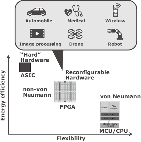
An FPGA is an integrated circuit on which it is possible to build processing blocks and processing flows that conform to the application by programming the internal circuit (hardware). This gives the FPGA a degree of flexibility comparable to a CPU. Because the FPGA performs information processing using non-von Neumann hardwired logic, it achieves higher processing capability than a von Neumann processor and is expected to play an increasingly important role in computing on the device side. Moreover, because the FPGA is a general-purpose circuit, it's not necessary to incur costs developing a new integrated circuit for each application.
While the FPGA offers a high degree of flexibility and powerful processing capability, it uses a semiconductor switch to change circuit configuration and incorporates a large amount of static random-access memory (SRAM) to memorize circuit configuration, thus increasing the circuit area and standby power. Because the SRAM requires power to retain data, standby power is inevitably consumed. This lowers the density of the logic circuits deployed for computing and increases the processing power in the unit of bits. This is an issue that needs to be addressed. Consequently, some research institutions at universities and various companies are now researching non-volatile memory that can replace the FPGA's SRAM and do not require data retention. Among the non-volatile memory under study are magnetoresistive random-access memory (MRAM)1) and resistive random-access memory (ReRAM)2)3).
2. NanoBridge Technology
To address the problems with the FPGA, NEC developed the NanoBridge, a non-volatile memory that can simultaneously replace both the semiconductor switch and semiconductor memory. The NanoBridge consists of a polymer-solid electrolyte (PSE) sandwiched between an inert electrode — ruthenium (Ru) — and an active electrode — copper (Cu) (Fig. 2)4). When positive voltage is applied to the copper electrode, the copper is ionized, shifting through the PSE to form a bridge between the two electrodes. As a result, the NanoBridge transitions from a high resistance (OFF) condition to a low resistance condition (ON). Conversely, when positive voltage is applied to the copper electrode, the copper atoms, which have formed the bridge, are retrieved by the copper electrode and transition to a high resistance condition.
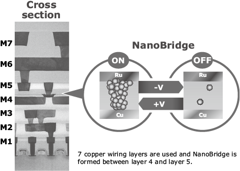
The NanoBridge can be rewritten repeatedly and does not require power to maintain ON and OFF conditions (non-volatile). Its electrical characteristics include smaller load capacity than the semiconductor switch (about 1/10th) and high ON/OFF resistance difference (500 Ω and 1 GΩ ). Therefore, the NanoBridge can function as a semiconductor memory to switch logic signals and retain circuit data. Moreover, because the thickness of the copper bridge is estimated to be just a few nanometers, it can be incorporated in a circuit even under a design rule with advanced integration.
When the NanoBridge is used in the NanoBridge-FPGA, two NanoBridges are connected facing each other and a write-controlling transistor is connected to an intermediate terminal on the ruthenium electrode side as shown on the lower right in Fig. 25). To switch the signal, both NanoBridges need to be in the ON or OFF condition. When operating voltage is applied to the switch in the OFF condition, the voltage stress is distributed between the two NanoBridges. Moreover, one of the two NanoBridges is placed so that it always achieves the voltage direction that allows for programming in the ON-OFF direction only. This complementarity improves reliability in the OFF condition, exponentially improving the retention lifetime under voltage stress. In addition, the program voltage — which is in a trade-off relationship with reliability in the OFF condition — can be suppressed because the circuit design allows individual NanoBridges to be programmed via intermediate nodes.
3. Architecture of the NanoBridge-FPGA
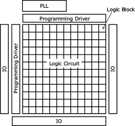
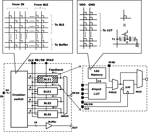
The basic NanoBridge-FPGA is configured with logic array blocks, input/output circuits that exchange logic signals with external components, a program driver for programming the NanoBridge, and a phase-locked loop (PLL) that generates clock signals (Fig. 3)6)7). Each logic block consists of four basic logic elements (BLEs) and a crossbar switch that determines where to connect the logic signals. Each BLE is comprised of a lookup table (LUT) where combinatorial logic operations are performed and D-type flip-flop (DFF) where sequential logic operations are executed. In Fig. 4 the NanoBridges are used in the crossbar switch and LUT memories. The crossbar switch is comprised of several NanoBridges. When any of the NanoBridges in each row is turned on, the output destination of the input signals of the logic block is determined. The output destination is selected from either the BLE or the adjacent logic block. Each LUT is equipped with sixteen memories. The value selected from the sixteen memories that has been chosen in accordance with the LUT's input signals is output. The memory of the LUT is also comprised of a NanoBridge. Once the NanoBridges composing the crossover switch and LUT are programmed to be ON or OFF, the circuit configuration is determined and the user application can be executed.
When the semiconductor memory or semiconductor switch — which is used for switching the LUT's memory and wiring — is replaced with a NanoBridge, the area of the logic block can be reduced. This means that the length of the wires used can also be reduced, further contributing to a reduction in power consumption.
4. Performance Evaluation of the NanoBridge-FPGA
To evaluate the performance of the NanoBridge-FPGA, we compared the NanoBridge-FPGA with a commercially available SRAM-based FPGA8) manufactured with a 40-nanometer semiconductor process9)10). As LUTs and DFFs are also used in the logic circuits of the SRAM-FPGA, the NanoBridge-FPGA and SRAM-FPGA can be compared based on the number of the LUTs. The density of the NanoBridge-FPGA's logic circuits fabricated in the same 40-nanometer semiconductor process is twice that of the SRAM-FPGA. Thus, when a NanoBridge is incorporated, the area occupied by the logic circuits can be reduced.
Both FPGAs were mapped with a benchmark circuit comprised of a 16-bit arithmetic logic unit (ALU) with a 1k-gate scale. The benchmark circuit includes an instruction decoder and an input signal generator. 332 LUTs and 73 DFFs are used in a single FPGA logic circuit. The count-up signals generated by a 16-bit counter — that have been mapped — are entered as operands of the ALU. Each of the 28 instructions is cyclically activated using a one-hot signal generator that has been mapped in the same manner.
The circuit configuration of the NanoBridge-FPGA is determined by programming the specified NanoBridge-FPGA to ON or OFF. NEC offers design tools to generate ON and OFF information from the application circuit. The application circuit is described at register-transfer level (RTL) and ON/OFF information can be generated using the fabricated FPGA tools7). First, a gate-level netlist is obtained using a logic synthesis tool according to the RTL description. The netlist is then converted into 4-input LUTs using a cluster packing tool. Further, the placement of the LUTs and their circuit connections are determined using a placement and routing tool to generate the circuit configuration information. The output signal pattern derived from the input signal pattern for the NanoBridge-FPGA implemented with an application circuit is generated by the Verilog test bench. Correct operation of the circuit can be verified using a semiconductor tester to see if the output signal pattern matches the operation of the NanoBridge-FPGA. We measured the operating voltage range, signal delay, and operating power using the semiconductor tester.
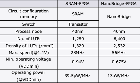
While the minimum operating voltage of the SRAM-FPGA is 0.94 V, the NanoBridge-FPGA can operate at voltages as low as 0.675 V. As for operating speed, the NanoBridge-FPGA runs twice as fast as the SRAM-FPGA at a standard operating voltage of 1.1 V. The SRAM-FPGA's dynamic power is 39.5 μW/MHz, while that of the NanoBridge-FPGA has been reduced by two-thirds to 13 μW/MHz (Table). These differences in performance are largely caused by the smaller load capacity of the NanoBridge, as well as the shorter wiring length made possible by the reduced size of the logic circuit's area, which reduces the load capacity in the wiring.
Table Performance comparison between the NanoBridge-FPGA and commercially available low power-consumption SRAM-FPGA.
5. Operation in Harsh Environments
IoT equipment is expected to be able to cope with harsh conditions and should be resistant to high temperatures and radiation.
Under high temperatures, the OFF current of a typical transistor changes exponentially with respect to the temperature. With the NanoBridge, however, changes in the OFF resistance can be suppressed and kept to a minimum. Hence, even in a high-temperature environment the NanoBridge needs less standby power than an SRAM-FPGA. Tests have confirmed that the NanoBridge-FPGA operates correctly at temperatures in the range of –50°C to 150°C11).
The NanoBridge is also resistant to radiation. An SRAM expresses ON and OFF conditions based on the number of charges. If high-energy radiation enters an integrated circuit that contains an SRAM, the radiation collides with silicon atoms on the semiconductor substrate, generating charges. These generated charges can disturb the charges on the SRAM, reversing the ON and OFF conditions and causing a malfunction. Since the NanoBridge achieves the ON/OFF condition based on the presence/absence of a physical copper bridge, the ON/OFF condition is not affected by radiation-generated charges.
We evaluated the NanoBridge’s resistance to radiation at the Heavy-Ion Irradiation Facility of the Japan Atomic Energy Agency. High-energy heavy ion (xenon and krypton ion) was irradiated on 128k NanoBridges to determine how it affected ON and OFF conditions. The linear energy transitions of the xenon and krypton are estimated to be 68.9 and 40.3 MeV/mg/cm² respectively. No changes were observed in the ON and OFF conditions before or after the ion irradiations. The NanoBridge’s ability to withstand radiation proved to be at least 100 times greater than flash memory which has a far higher resistance to radiation than SRAM.
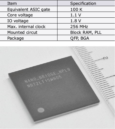
We plan to subject the NanoBridge-FPGA to in-orbit testing via the Innovative Satellite Technology Demonstration Program of the Japan Aerospace Exploration Agency (JAXA) in FY 201812). The NanoBridge-FPGA will to be inserted into orbit by the Epsilon rocket in FY 2018. Fig. 5 shows the specifications of the NanoBridge-FPGA which will be used in the in-orbit evaluation. We will employ an image compression application and radiation durability testing circuit on the FPGA. We plan to use the NanoBridge-FPGA to compress full-HD images captured by the satellite camera and downlink the images to the ground station for fault evaluation. We have written the above-mentioned circuits onto the NanoBridge-FPGA and have already conducted various ground tests, including heat cycle testing and vibration testing, to confirm that the NanoBridge’s ON/OFF conditions do not change. This program is being conducted in collaboration with the JAXA.
6. Conclusion
The low-power non-volatile FPGA has been verified for applications in devices with limited usable power. The FPGA combined with the NanoBridge for the wiring switch and LUT memory features twice the logic density, twice the operation speed, and three times the dynamic power as a conventional SRAM-based FPGA manufactured using the same 40-nanometer node technology. The NanoBridge-FPGA we have developed is ideal for high-performance and low-power consumption computing in edge devices.
7. Acknowledgements
The above results, which are part of a larger study, have been obtained in "Development of One Million LUT Atom Switch FPGA," which is a program subsidized by the New Energy and Industrial Technology Development Organization (NEDO). We would also like to express our gratitude for the cooperation we received in the creation of device prototypes from the Super Clean Room Station, Open Research Platform Unit, TIA Central Office, National Institute of Advanced Industrial Science and Technology (AIST).
Reference
- 1) Daisuke Suzuki et al.: Fabrication of a 3000-6-input-LUTs embedded and block-level power-gated nonvolatile FPGA chip using p-MTJ-based logic-in-memory structure, VLSI Technology, 2015
- 2) Young Yang Liauw et al.: Nonvolatile 3D-FPGA with monolithically stacked RRAM-based configuration memory, Solid-State Circuits Conference Digest of Technical Papers (ISSCC), 2012
- 3)
- 4) Munehiro Tada et al.: Polymer solid-electrolyte switch embedded on CMOS for nonvolatile crossbar switch, I IEEE Transactions on Electron Devices, Volume 58, Issue 12, pp.4398-4406, December 2011
- 5) Munehiro Tada et al.: Highly reliable, complementary atom switch (CAS) with low programming voltage embedded in Cu BEOL for Nonvolatile Programmable Logic, Electron Devices Meeting (IEDM), 2011
- 6) Makoto Miyamura et al.: Low-power programmable- logic cell arrays using nonvolatile complementary atom switch, Quality Electronics Design (ISQED), 2014
- 7) Makoto Miyamura et al.: 0.5-V Highly Power-Efficient Programmable Logic using Nonvolatile Configuration Switch in BEOL, 2015 ACM/SIGDA International Symposium on Field-Programmable Gate Arrays, pp.236-239, 2015
- 8)
- 9) Yukihide Tsuji et al.: A 2× logic density Programmable Logic array using atom switch fully implemented with logic transistors at 40nm-node and beyond, VLSI Circuits, pp. 16-17, June 2016
- 10) Xu Bai et al.: A low-power Cu atom switch programmable logic fabricated in a 40nm-node CMOS technology, VLSI Technology, June 2017
- 11) Makoto Miyamura et al.: NanoBridge-Based FPGA in High- Temperature Environments, IEEE Micro, Volume 37, Issue 5, pp.32-42, October 2017
- 12)
 Kazuya Terabe et al.: Quantized conductance atom switch, Nature 433, pp. 47-50, January 2005
Authors' Profiles
SAKAMOTO Toshitsugu
Principal Researcher
System Platform Research Laboratories
Principal Researcher
System Platform Research Laboratories
MIYAMURA Makoto
Principal Researcher
System Platform Research Laboratories
Principal Researcher
System Platform Research Laboratories
BAI Xu
Assistant Manager
System Platform Research Laboratories
Assistant Manager
System Platform Research Laboratories
SUGIBAYASHI Tadahiko
Senior Engineer
System Platform Research Laboratories
Senior Engineer
System Platform Research Laboratories
TADA Munehiro
Principal Researcher
System Platform Research Laboratories
Principal Researcher
System Platform Research Laboratories