
Global Site
Breadcrumb navigation
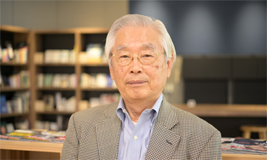
The Discovery and Future of Carbon Nanotubes Sumio Iijima
September 24, 2024

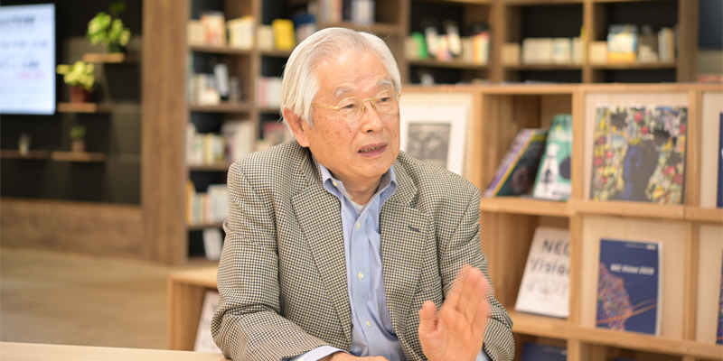
As one of the materials that support nanotechnology, carbon nanotubes have been gathering global attention. Dr. Sumio Iijima, an NEC Senior Research Fellow, has continued, to this date, to take an active role in research activities since his discovery of this material. We interviewed Dr. Iijima about his most recent research and future prospects.
Senior Research Fellow
Sumio Iijima
After engaging in research at Tohoku University, Arizona State University, University of Cambridge, and Research Development Corporation of Japan (now Japan Science and Technology Agency), he joined NEC Corporation in 1987. Using an electron microscope, in 1991 he discovered carbon nanotubes, a fourth-allotrope carbon solid (*1) that became a focus of international attention. Dr. Iijima is currently a University Professor of Meijo University, Honorary AIST Fellow of National Institute of Advanced Industrial Science and Technology (AIST) and a Distinguished Invited University Professor of Nagoya University.
The Challenge to Mass-produce Carbon Nanotubes and Electrode Materials for Solid-state Lithium-ion Batteries
― What activities are you engaged in currently?
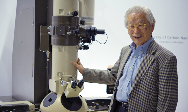
My area of research is electron microscopes, and I am tackling the scientific challenges that still remain unresolved today in this field.
For example, a substance I was studying 40 to 50 years ago is now being intensely researched as an electrode material for solid-state lithium-ion batteries. It is an oxide used as an electrode material. There is no reason that I shouldn't work on this, so I am currently trying to unlock and explain the basic crystal structure of this material. Once we know the crystal structure, the possibility of practical application to solid-state lithium-ion batteries opens up. While a prior study of the crystal structure was conducted at a large-scale research facility using the neutron diffraction approach, interestingly, similar results are produced recently using an electron microscope. This is not merely a matter of understanding the crystal structure of this material, but is also a question that implicates the two different approaches, namely neutron diffraction and electron microscopes, making for a universal and very interesting research finding. It is quite fascinating to compete against a neutron-based study using a 10-billion-yen facility with an electron microscope that costs around 500 million yen. The previous findings have been organized into research papers and submitted to science journals.
I am still engaged in research into carbon nanotubes. The area of carbon nanotubes is still left with the most difficult problem barring the way to practical use. It is the mass production issue that is being an obstacle to using them in electronic devices. Semiconductors and transistors that use carbon nanotubes are said to outperform their currently mainstream silicon counterparts. Nevertheless, for practical application as a material taking over from silicon, carbon nanotubes must be mass-producible in units of millions. To make that a reality, we need a technique that orients and aligns the tangled weaves of just-created carbon nanotubes in the same direction. This is a challenge that many have previously tried their hand at, and no one has yet succeeded. I have been working on this issue for about two years. I carried out a preliminary experiment with a method that I came up with last year and filed a patent application.
The solution to truly arduous problem for which clues do not come with just time spent should be left for senior researchers with abundant experience like us to work on. It’s also a purpose of my life to break grounds for nanomaterials and nanoscience. And most of all, research is fun. *Laugh*
Pure and applied research in material science are two sides of the same coin
― Do you consider applied research and practical application important?
Material research is only valuable when it becomes useful to the society. First of all, pure and applied research in the field of material science are inextricably linked together. That is also what makes this area of study very interesting.
Taking the invention of semiconductor for an example, the basic research into nanomaterials has played a tremendous part. Right after joining NEC, I myself observed a compound semiconductor made of indium gallium phosphide using an electron microscope and became the first in the world to discover the alternating orderly alignment it of the atoms. The discovery defied the conventional belief that atoms are chaotically bunched in such a compound. Once you know the structure of a material, then the policy on how it should be used changes, affecting the performance of the semiconductor. Like this, the atomic and molecular information that electron microscopes provide has been directly useful for finding the answers to the industrial questions of how to create something with better performance or durability. Notably in Japan in the 1960s, there was close coordination between the development of iron and steel industry and the research on iron crystals.
When pure research progresses, so does the industries using the research findings. That playing catch between the industry and academics functions well for mutual benefits—the ability to build an even closer relationship than other fields of study is one of the things that makes material research intriguing.
The real achievement comes from experience and coincidence
― Do you have any future goals?
No, not any more. *Laugh* Besides, there is no knowing what I will do next. For an “experimenter” like me, ideas for what to do next do not come just by reading some literature or accessing new information. Most research comes about incidentally based on previous experiences. In fact, the real achievement cannot be achieved otherwise. What I mentioned in the beginning where I said that a material that I studied 40 to 50 years ago only recently started being researched as a material with potential is a good example of this.
However, this does not apply to “theorists” like Hideki Yukawa, Shinichiro Tomonaga, and Kenichi Fuku, who are Nobel prize laureates. An ordinary person like myself should not set foot in the realm of such geniuses. A theorist can establish a theory by intending to do something new from the very start, but we, the experimenters, cannot do something by envisioning it from the beginning. When you try doing this, you find something better here. You try doing something here, and then you come across something even better there... It is this endless repetition of trial and error that lets us stumble on serendipity, the fortuitous discovery.
So I am fond of saying that even laymen can do science. Many of Nobel Prize-worth inventions came about from coincidences. Doesn't this fact give us great courage that even people like us can do science?
- (*1) Allotropes of carbon
1. Graphite, 2. Diamond, 3. Fullerene, 4. Carbon nanotubes, 5. Graphene
Related Link